Table of Contents
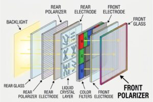
Flexible Printed Circuits (FPCs) serve as the critical connective tissue in modern LCD modules, enabling sleek, lightweight, and high-performance displays across industries from consumer electronics to automotive systems. By integrating thin, bendable copper traces and robust adhesives, FPCs provide seamless connectivity between an LCD’s driver IC, backlight unit, and external circuits while conserving space and enhancing durability. Their ability to withstand dynamic bending and thermal stress makes them indispensable for compact designs like smartphone screens, curved TVs, and wearable devices.
However, optimizing FPC layouts—such as managing electromagnetic interference (EMI) in MIPI differential signals, balancing trace impedance, and ensuring reliable power delivery—is essential to unlocking the full potential of LCD modules. This guide explores the symbiotic relationship between FPC design principles and LCD functionality, offering actionable insights for engineers seeking to balance innovation with manufacturability.
Part 1: Fundamentals of FPC
1. FPC Materials and Classification
a) Copper Foil Types
- Rolled Annealed Copper (RA): Superior mechanical flexibility; ideal for applications requiring repeated bending.
- Electrodeposited Copper (ED): Better suited for fine-pitch (<0.2mm) designs.
- Thickness Options:
- 1/3 oz (12μm)
- 1/2 oz (18μm) [Standard at our company]
- 1 oz (36μm)
b) Substrate Materials
- PI (Polyimide): Higher cost but excellent flame resistance (preferred for soldering processes).
- PET (Polyester): Lower cost but poor heat tolerance.
c) Manufacturing Processes
- Single-Sided vs. Double-Sided: Determined by circuit complexity.
- Laminated vs. Non-Laminated: Laminated substrates offer enhanced durability.
2. FPC Structure
Double-Sided Laminated FPC
Cover Film + Copper Foil + Substrate + AD Thermosetting Adhesive Film


Single-Sided Laminated FPC
Cover Film + Copper Foil + Substrate

Part 2: FPC Anti-Interference Routing Design
1. MIPI Differential Signal Routing
Key Guidelines:
- Avoid parallel or angled crossings with other signals; prioritize perpendicular routing.

- Add ground shielding along FPC edges to reduce edge radiation.

- Ensure continuous ground reference planes beneath MIPI traces (minimum 4× trace width clearance)

- Maintain pair-to-pair length matching:
- within-pair skew: ≤10mil
- Inter-pair skew: ≤200mil
- Use full ground plane coverage around signal traces.

2. Power/Ground Routing Optimization
Ground (GND) Routing
- Continuity: Avoid fragmented ground pours.

- Fine-Pitch Design: Group GND traces and widen connections (see diagram below).

- Via Density: Increase ground vias in high-density areas to improve interlayer connectivity.

Power (VDD) Routing
- Input Traces: ≥0.2mm width for stability.
- Isolation: Separate DRIVER IC and booster IC power paths.

- Filtering: Add 2.2μF/6.3V capacitors near DRIVER IC inputs.

- Via Strategy:
- Dense via stitching on VDD layers.
- Adjacent ground vias to reduce impedance.

Best Practices Summary
| Category | Priority Action Items |
| Signal Integrity | Prioritize ground shielding; control trace lengths. |
| Thermal Management | Optimize copper thickness (1/2oz standard). |
| Manufacturability | Simplify complex bends; avoid over-via density. |


-300x300.jpg)
-300x300.jpg)