Introduction to AMOLED
AMOLED (Active Matrix Organic Light Emitting Diode) is a type of active-matrix OLED display panel. Compared with traditional LCD panels, AMOLED offers faster response times, higher contrast ratios, and wider viewing angles.
In terms of image quality, power efficiency, and long-term cost potential, AMOLED has inherent advantages over TFT LCD. This is why many major global manufacturers continue to invest heavily in improving yield rates rather than abandoning AMOLED development.
From a performance perspective, AMOLED panels outperform TFT LCDs due to their fast response, superior contrast, and wide viewing angles. In addition, AMOLED displays are self-emissive and do not require a backlight module, enabling much thinner designs. Power consumption is another key advantage: current AMOLED panels consume roughly 50% less power than TFT LCDs, with further reductions expected as technology advances.
Perhaps even more importantly, eliminating the backlight module allows AMOLED displays to save 30–40% of the total cost typically attributed to the backlight in TFT LCD panels.

Thanks to these advantages—vivid color performance, low power consumption, and slim form factors—AMOLED has become the preferred choice for mainstream consumer electronics, including smartphones (such as iPhone and Huawei devices), tablets, and even high-end television models.
However, the biggest challenge for AMOLED remains manufacturing yield. At present, AMOLED panels are still significantly more expensive than TFT LCDs, which creates a major barrier to large-scale adoption.
Currently, AMOLED technologies can be broadly divided into six main categories, as outlined below.
1. Metal Oxide TFT Technology
Metal oxide TFT technology is widely regarded by manufacturers and industry research firms as a promising solution for large-sized AMOLED displays. Many companies have already demonstrated large-panel prototypes based on this approach.
The TFT backplane in this technology uses mature large-area sputtering deposition processes common in the LCD industry. The oxide semiconductor material is typically InGaO₃(ZnO)₅. Although its electron mobility (~10 cm²/V·s) is lower than that of LTPS, it is more than 10 times higher than amorphous silicon, making it fully sufficient for OLED current driving requirements.
At present, metal oxide TFT technology is still in the laboratory validation stage. There is no large-scale mass production experience yet, mainly due to unresolved issues related to process reproducibility and long-term operational stability.
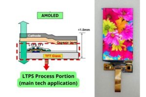
2. Low-Temperature Polycrystalline Silicon (LTPS) TFT Technology
LTPS TFT technology is currently the only AMOLED backplane technology that has been fully validated through commercial mass production, especially on Gen 4.5 and smaller production lines.
The key difference between LTPS and amorphous silicon technology lies in the use of laser crystallization, which transforms amorphous silicon into polycrystalline silicon. This increases electron mobility from around 0.5 cm²/V·s to 50–100 cm²/V·s, fully meeting OLED current driving requirements.
After years of mass production, LTPS AMOLED displays have demonstrated excellent performance and high operational stability. Yield rates have increased significantly, reaching approximately 90%, which has greatly reduced production costs.
From a process perspective, LTPS mainly differs from a-Si in the addition of laser crystallization and ion implantation steps. Most other processes and equipment are similar and compatible with conventional a-Si TFT production lines.
Several crystallization methods exist, including:
- ELA (Excimer Laser Annealing) – most common for small panels
- SLS
- YLA
Some companies are also exploring metal-induced crystallization, but this approach faces major challenges. Metal contamination can cause interlayer dielectric breakdown and high leakage currents, making long-term device stability difficult to guarantee—particularly critical for ultra-thin AMOLED structures.
Key Limitations of LTPS:
- Complex manufacturing process requiring 6–9 photomasks, leading to high initial equipment costs
- Limited scalability to large sizes due to laser crystallization constraints (currently up to Gen 4.5)
- Laser crystallization can cause mura effects, making it unsuitable for large TV panels
3. Amorphous Silicon (a-Si) TFT Technology
Amorphous silicon TFT technology is the most widely used approach in LCD manufacturing today. Except for a few LTPS-based lines, most LCD factories rely on a-Si technology.
a-Si TFTs feature a simple device structure, typically 1T1C (one TFT and one storage capacitor). Manufacturing usually requires 4–5 photomasks, with some manufacturers developing 3-mask processes.
One major advantage of using a-Si for AMOLED production is that existing LCD TFT equipment can be reused, resulting in low initial capital investment. In addition, a-Si technology has already proven its scalability, supporting LCD panels larger than 100 inches.
However, OLED devices are current-driven, while a-Si TFTs have very low electron mobility, making them unsuitable for driving OLED pixels. Some companies (e.g., Ignis in Canada) have attempted to address this through IC design improvements, but these solutions do not fundamentally solve the problem.
Another significant challenge is the lack of compatible driver ICs. Most IC vendors focus on LTPS-based designs, resulting in limited support for a-Si AMOLED solutions. As a result, performance is compromised and supply chains become constrained.
4. Microcrystalline Silicon TFT Technology
Microcrystalline silicon TFT technology is similar to conventional a-Si TFTs in terms of materials and layer structure.
Its electron mobility ranges from 1–10 cm²/V·s, and it has been adopted by Sony in certain applications. While this mobility is sufficient to drive OLEDs, overall display performance is limited. Due to its relatively low efficiency and inferior image quality, few manufacturers actively pursue this technology.
Comparative Summary of TFT Technologies
- LTPS TFT
- Very high electron mobility
- Fully meets OLED driving requirements
- High yield (~90%) and mature mass production
- High cost and limited scalability
- Metal Oxide TFT
- Adequate mobility for OLED driving
- Easier large-scale scalability
- Stability and mass-production maturity remain challenges
- a-Si and Microcrystalline Silicon TFTs
- Simple processes and low initial costs
- Suitable for voltage-driven LCDs
- Poor fit for current-driven OLEDs
Based on current global AMOLED manufacturing practices and the above analysis, LTPS TFT technology using laser crystallization remains the most practical choice today. At the same time, metal-induced crystallization should be encouraged as a future research direction.
5. Organic Layer Deposition Technology
Organic layer formation methods can be divided into traditional vapor deposition and emerging transfer/printing techniques.
- Transfer technology: Jointly developed by Samsung and 3M
- Printing technology: Developed primarily by Epson

These new approaches improve material utilization and simplify processes, but they are currently limited by proprietary materials and lack mass-production capability.
Traditional vapor deposition methods include:
- Point-source evaporation
- Line-source evaporation
- OVPD (Organic Vapor Phase Deposition)
OVPD, developed by Aixtron (Germany), offers improved manufacturability, better uniformity, precise doping control, and higher process stability. It also reduces maintenance requirements and material waste.
However, OVPD currently faces two limitations:
- Mature equipment supports only 370 × 470 mm substrates
- Reliability for full-color devices remains insufficient
As a result, point-source and line-source evaporation remain the primary production methods today. TOKKI (Japan) leads in point-source systems, while ULVAC (Japan) excels in line-source systems.
6. Light Emission Direction: Bottom vs. Top Emission
OLED devices can be classified into bottom-emission and top-emission structures.

- Bottom emission
- Mature process
- Low risk
- Lower technical difficulty
- Top emission
- More complex cathode fabrication
- Challenging encapsulation process
- Represents a future trend, especially for higher aperture ratios

In general:
- a-Si backplanes are better suited for top-emission OLEDs
- Poly-Si (LTPS) backplanes can adopt bottom-emission designs
If future breakthroughs significantly improve backplane mobility and uniformity, bottom-emission OLEDs may offer even greater cost advantages.