Currently, many high-end smartphones are equipped with AMOLED displays. Although the term AMOLED is frequently mentioned, do you really understand its relationship with OLED? Why are smartphone manufacturers racing to secure OLED panels? Can smartphones and VR devices push OLED into becoming the mainstream display technology?
With these questions in mind, let’s take a comprehensive look at OLED technology.
OLED Structure and Light-Emitting Principle
Organic Light-Emitting Diode (OLED) is a display technology originally developed and patented by Kodak. This technology uses organic polymer materials as the semiconductor materials in light-emitting diodes. These polymers can be natural or synthetically produced, large or small in molecular size. Proteins and DNA are examples of organic polymers.

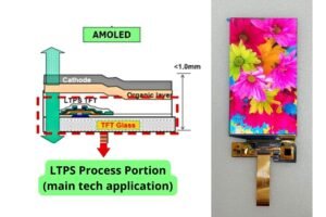
The basic OLED structure resembles a sandwich, consisting of an ITO (Indium Tin Oxide) layer connected to the positive electrode, combined with a metal cathode. The layered structure includes a hole transport layer, an emissive layer, and an electron transport layer.
Under the influence of an electric field, holes generated by the anode and electrons generated by the cathode move toward the hole transport layer and electron transport layer, respectively, and are injected into the emissive layer. When electrons and holes meet in the emissive layer, excitons are formed, which excite the light-emitting molecules to produce visible light.
When the applied voltage reaches an appropriate level, holes from the anode combine with electrons from the cathode in the emissive layer, producing light. Depending on the material formulation, red, green, or blue light is emitted, which then forms full-color images based on the RGB color-mixing principle.
OLED vs. LCD
OLED displays are self-emissive, meaning each pixel emits its own light. In contrast, LCDs do not emit light and require a backlight source beneath the panel.
An LCD module (LCM) consists of the LCD panel and the backlight unit. The LCD panel typically includes polarizers, glass substrates, color filters, transparent electrodes, TFTs, and liquid crystals. The backlight unit includes light sources, light guide plates, optical films, and structural components.
OLED Classification and Characteristics

Based on driving methods, OLED displays can be divided into:
- PMOLED (Passive Matrix OLED)
- AMOLED (Active Matrix OLED)
PMOLED
PMOLED uses a matrix formed by cathodes and anodes, lighting pixels through a scanning method. Each pixel operates in pulse mode, emitting high brightness momentarily.
Advantages: Simple manufacturing process, lower cost
Disadvantages: Not suitable for large-sized or high-resolution displays
AMOLED
AMOLED uses independent TFTs to control each pixel. Each pixel can emit light continuously and independently.
Advantages: Low driving voltage, longer lifespan of light-emitting components
Disadvantages: Complex manufacturing process, difficult cost control
AMOLED occupies the vast majority of the OLED market and represents the mainstream development direction. In today’s market, when people refer to “OLED displays,” they generally mean AMOLED.
Key Advantages of OLED Technology
- Ultra-thin structure, approximately one-third the thickness of LCDs
- Solid-state components with strong shock resistance
- Wide viewing angles with minimal color shift
- Faster response times compared to LCDs (up to 1000× faster in early OLED TVs like Sony’s 11-inch XEL-1 released in 2007)
- Excellent low-temperature performance (operational even below -75°C if circuitry is intact)
- Higher energy efficiency compared to LCDs
- Can be fabricated on various substrates, including flexible materials
Although early OLED displays suffered from limited lifespan, significant improvements in recent years have enabled widespread adoption in mobile phones. However, OLED panels remain more expensive than LCDs, and further breakthroughs in mass production are still needed.
AMOLED Manufacturing Process
Since AMOLED dominates the OLED market, we focus on its production process:
Backplane Process → Frontplane Process → Module Assembly
Backplane Process
The first step in both AMOLED and TFT-LCD production is the fabrication of the TFT backplane.
OLED is a current-driven device and requires highly stable current, which depends on carrier mobility. Therefore, LTPS (Low-Temperature Polycrystalline Silicon) is the most suitable semiconductor thin film for OLED TFTs. Most AMOLED panels use LTPS substrates, while LCDs commonly use a-Si due to cost and process considerations.
Key differences between TFT usage in LCD and OLED:
- LCD pixels require only one TFT, while OLED pixels require at least four TFTs.
- OLED TFTs require much higher manufacturing precision, resulting in lower yields.
The backplane process involves film deposition, photolithography, and etching to form LTPS structures, with micron-level precision and extremely high uniformity requirements.
Key equipment includes:
- Photolithography systems
- Wet and dry etching machines
- ICP etchers
- PVD and CVD systems
- Laser crystallization systems
- Ion implantation machines
- Rapid thermal annealing equipment
Frontplane Process
The frontplane process is the most critical stage in AMOLED manufacturing.
After cleaning and drying, the LTPS-TFT substrate is transferred into a nitrogen environment for cooling and flipped so the film side faces downward. The substrate is then placed in a high-vacuum chamber (approximately 5×10⁻⁵ MPa) for evaporation of functional layers and emissive layers.
After deposition, the panel undergoes functional and visual inspection, polarizer attachment, and then proceeds to module assembly.
Key equipment includes:
- Substrate transfer systems
- Cleaning equipment
- Evaporation machines
- Tensioning machines
- Aging and curing systems
The core of AMOLED manufacturing lies in vacuum evaporation, where organic materials and metal electrodes are deposited onto the LTPS substrate. This process requires extremely specialized equipment.
Currently, Canon Tokki (a Canon subsidiary) is widely recognized as the global leader in OLED evaporation equipment and holds a near-monopoly in large-scale mass production tools.
Module Assembly Process
The final stage involves assembling the AMOLED panel into a usable module.
Compared to LCD modules, AMOLED modules are simpler because they do not require backlight units or color filters.
The basic steps include:
- Panel cutting, cleaning, and drying
- ACF attachment
- COG, FOG, and TAB bonding
- Electrical testing
- Protective coating and curing
- Final assembly and packaging
Key equipment includes:
- Cleaning machines
- Cutting machines
- ACF bonding machines
- COG/FOG/OLB bonding equipment
- Aging test systems
- AOI inspection systems
Technical and Application Challenges of OLED
OLED is widely regarded as the future of display technology. However, large-size OLED panels—especially those using oxide TFT technology—face significant challenges related to yield, cost, and scalability.
Key obstacles include:
- Large-size panel fabrication
- Organic material deposition uniformity
- Encapsulation reliability
Large-Size OLED Panel Challenges
LTPS processes struggle beyond Gen 5.5 production lines due to limitations of RGB horizontal evaporation using fine metal masks (FMM). As panel sizes increase, gravity causes mask sagging, leading to color mixing and reduced resolution.

Oxide TFT Technology Considerations
Common oxide TFT structures include:
- Coplanar
- Etch Stop Layer (ESL)
- Back Channel Etch (BCE)
While coplanar structures are simpler, they suffer from reliability issues. BCE and ESL structures offer better performance and yield, with ESL providing the highest reliability at the cost of process complexity.
Oxide TFTs are sensitive to light and heat, causing threshold voltage shifts, which complicates process stability and uniformity.

OLED Color and Deposition Challenges
OLED displays use RGB subpixels deposited via vacuum evaporation. Maintaining uniform brightness and color balance becomes increasingly difficult as panel size increases. Blue OLED materials have shorter lifespans, requiring compensation that can distort color accuracy.

Curved and White OLED Displays
Tandem OLED structures have enabled high-efficiency white OLEDs suitable for lighting and displays. However, white OLEDs lag behind RGB OLEDs in color gamut and purity and require over ten thin-film layers, demanding extremely high thickness uniformity.
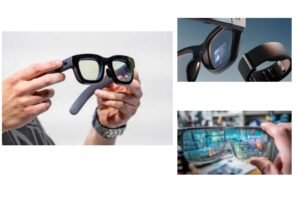
Future Outlook and Competing Display Technologies
OLED, MicroLED, and QLED are considered next-generation display technologies. All three use self-emissive RGB subpixels and can theoretically achieve up to 95% light efficiency.
From a manufacturing perspective, these technologies share approximately 70% of their equipment and processes, making competition less “winner-takes-all” than past LCD vs. plasma battles.
Technology Comparison
- OLED: Mature ecosystem, flexible, but limited lifespan and stability
- QLED: Inorganic materials with excellent longevity, but difficult large-scale manufacturing
- MicroLED: Highest efficiency and brightness potential, but extremely challenging mass transfer and assembly processes
MicroLED offers superior energy efficiency and brightness density, requiring only ~10% of the emissive area compared to OLED for the same brightness.
Ultimately, the future winner among OLED, MicroLED, and QLED will not be determined solely by performance metrics, but by engineering feasibility, manufacturing yield, cost efficiency, and long-term reliability under large-scale production.
OLED, despite its limitations, already meets the practical requirements of consumer electronics and remains a dominant force in today’s display industry.

")